Semiconductor processing technology Unit
The unit possesses this key equipment for processing semiconductor devices and their prototyping.
- The substrate preparation and chemical formation of structures are made by:
– Wet chemical etching,
– Electrochemical etching,
– Chemical polishing,
– Surface cleaning.
- The coatings, substrates, devices and the prototypes of new structures are thermally treated by
– Hot plates and baking systems with / without controlled atmosphere,
– Rapid annealing furnace (UniTemp),,
– Tube furnaces with vacuum and up to 4 channels gas delivery and control systems,
– Three-zone tube furnaces with controlled zone temperatures and gas atmosphere.
- The thin film deposition and metallisation systems are mainly based on the physical vapour deposition methods. For the PVD solid film growth we use:
– Vacuum system for thermal evaporation,
– DC-magnetron sputtering system acceptable for the film growth in pure argon and reactive gas atmospheres,
– RF-magnetron sputtering system,
– multi-mode magnetron sputtering system that can be operated in the DC-, RF- and Power Impulse modes with the co-sputtering and controlled atmosphere,
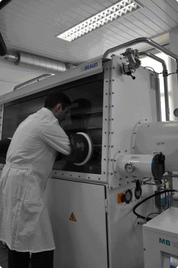
– e-beam sputtering system (MB 200B, VST).
- The manufacture and characterization of microstructures are performed by means of -conventional photolithography and the laser lithography systems. We are using the following systems:
– Standard lithography processing in proximity exposure mode for wafers up to 100 mm,
– Laser lithography system for high resolution pattern generation acceptable for low volume mask making and direct writing,
– High resolution optical microscopes with the CCD camera,
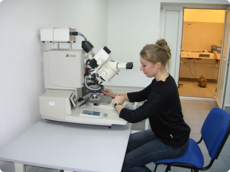
– Scanning probe microscope (SPM) with the topography, electrical and magnetic imaging of the surfaces also with the force and the tunneling current spectroscopy; the XY resolution is better than 0.5 A, the Z resolution is better than 0.1 A, the tunneling current resolution is better than 0.1 pA.
- Manufacturing of semiconductor devices and the prototypes includes a splitting of batches of elements formed on a substrate, assemblage and encapsulation within the standard and original frames. For these processes we use:
– Diamond Scriber acceptable for fast, easy and precise scribing and cutting of silicon wafers, as well as thin- and thick film ceramic and glass substrates,
– Thermocompression bonding and capacitive discharge spot welder.
- Characterisation of the elements and assembled devices are characterized and tested in a probe station with the set-up for measurement of the main electrical characteristics I-V and C-V in the dc-current, ac-current and pulsed-current modes.