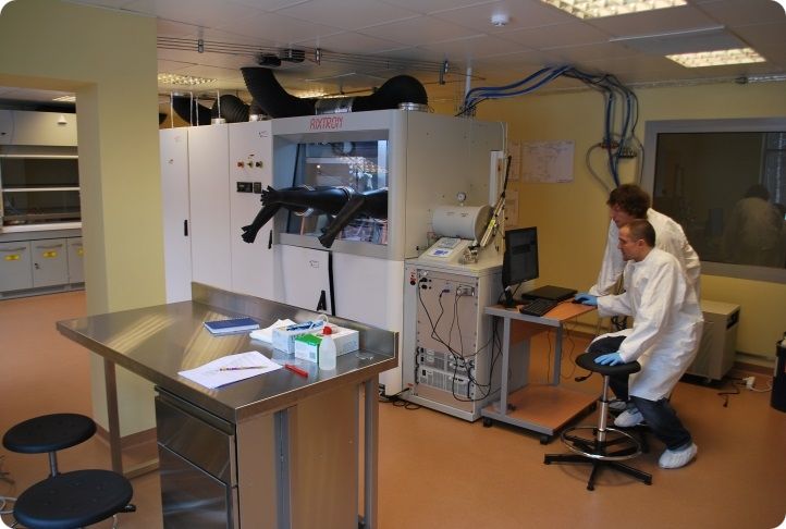
Epitaxial Semiconductor Technology Unit
Epitaxy of III-nitride semiconductor structures by MOCVD technology
- Growth of group III-nitride films (GaN, AlN, InN, AlGaN, InGaN, InAlN, BGaN) by MOCVD on sapphire, Si, SiC, and bulk GaN wafers;
- Growth of structures for high-power electronic and optoelectronic devices (LED, field-effect transistors, solar cells, diodes, sensors);
- Surface analysis using optical microscope and Scanning Electron Microscope (SEM);
- Study of the structures by Electron Beam-Induced Current (EBIC) measurement device;
- Elemental analysis and/or mapping of chemical composition in the material by Energy-Dispersive X-ray Spectroscopy device (EDS or EDX),
- Reactive Ion Etching (RIE) and Rapid Thermal Annealing (RTA) facility.
Technical details of the epilayers and structure
- Unintentionally doped GaN (uGaN), minimal carrier densityne=1016 cm-3, electron mobility µe =250 cm2/Vs, , growth speed 0.1¸2.5 mm/h, maximum layer thickness up to 15 mm.
- n-typeGaN doped with Si, ne =1016¸1018 cm-3, me=150¸250 cm2/Vs; growth speed 1¸2.5 mm/h.
- p-typeGaN doped with Mg, nh=1016¸1018 cm-3, me=5¸10 cm2/Vs, growth speed 0.5¸2 mm/h.
- InGaN: In content from 1% up to 25%, and from 60% to 99%, minimal ne =1017¸1020 cm-3, me =100¸230, mobility depends on Incontent, growth speed 50¸200 nm/h, possible doping with Si and Mg.
- InN:ne =1018¸1020 cm-3, me=600 cm2/Vs, growth speed 10¸100 nm/h.
- AlGaN: Al content from 1% up to 100% (AlN), growth speed 0,05¸1 mm/h, crack-free layers can be grown from 1¸2 nm up to 1 mm.
- Growth of BGaN under development.
Contact person:dr. Roland Tomašiūnas; Ph: +370-52366079,
e-mail: rolandas.tomasiunas@ff.vu.lt
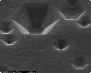
MOCVD reactor SEM picture of GaN epilayer surface
Contact person:dr. Roland Tomašiūnas; Ph: +370-52366079,
e-mail: rolandas.tomasiunas@ff.vu.lt
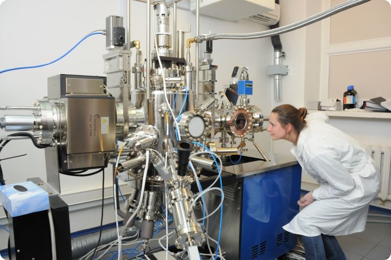
MBE growth technology
- Molecular beam epitaxy reactor SVT-A,
- 7 solid state sources (Ga, Al, In, As, Bi, Si, Be),
- Growth on GaAs and InP substrates,
- Material systems: AlGaAs, GaInAs, AlInAs, GaAsBi, AlAsBi, GaInAsBi, AlGaAsBi,
- Semiconductors with subpicosecond carrier lifetimes: LTG GaAs, LTG InGaAs,
- Quantum wells and superlattices,
- Device structures: ultrafast photoconductors for THz radiation emission and detection, light-emitting and laser diodes, uni-travelling-carrier photodiodes, semiconductor saturable absorber mirrors.
- Another MBE machine is planned of being acquired in 2014.
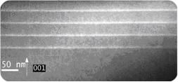
5nm thick GaAsBi quantum wells with GaAs barriers (TEM image)