Technology of the Organic Semiconductor Structures Unit
Technology laboratory for deposition of organic, organic-inorganic hybrid layers using various deposition technologies: spin-coating, casting, doctor blade, spraying, and thermal deposition in vacuum.
Technological equipment
Basic setup for sample preparation and incapsulation:
- fume hood,
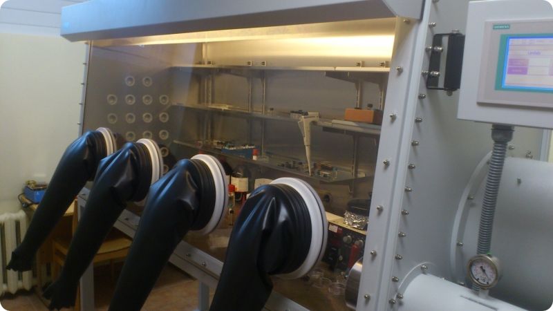
- 4 glove glovebox (with connections for electrical measurements),
- spincoaters, hotstage inside and outside glovebox.
HiCube Turbo pumping stage for evaporation of electrodes outside glovebox.
Setup for deposition of the organic layers with following metallization, complete fabrication and encapsulation under nitrogen atmosphere:
- 8 glove glovebox system with vacuum deposition system inside.
- spincoaters and hotstage inside and outside glovebox,
- system of substrate cleaning in oxigen plasma,
- system of sample annealing in nitrogen atmosphere or vacuum.
Vacuum deposition system with 5 thermal evaporators (3 for evaporation of organic materials and 2 for evaporation of metals), shutters, and layer thickness control.
Primary characterization equipment
- Atomic force microscope;
- Polarized light microscope;
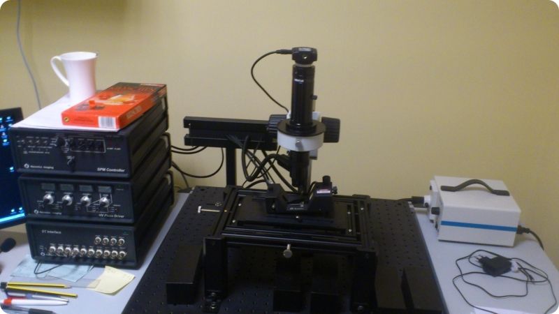
- Scanned probe microscopy system Nanonics Multiview 1000:
- contact, non contact, intermittent contact modes,
- up to 100 microns in X, Y and Z axis,
- sample size: up to 16 mm,
- resolution: XY: 0.005 nm; Z: 0.002 nm
- I-V measurement systems;
- Time-of-flight (TOF) measurement system;
- Charge Extraction by Linearly Increasing Voltage (CELIV) measurement system;
- Modified CELIV (photo-CELIV, i-CELIV, CEPV) measurement systems.
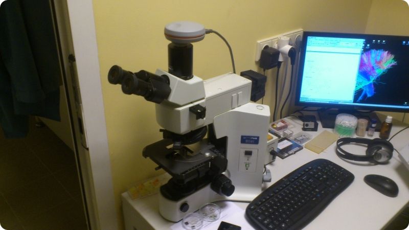
Atomic Force Microscope Polarized Light Microscope
Contact person: prof. Kestutis Arlauskas; e-mail: kestutis.arlauskas@ff.vu.lt
Under installation
Organic Electronic Device Fabrication Facility
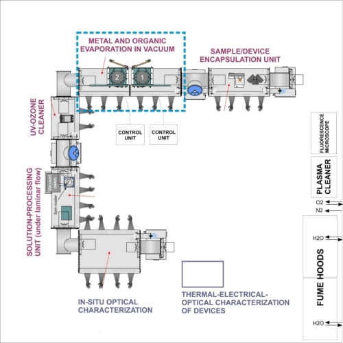
Organic electronic device fabrication facility (currently being installed)
The system is designed for the research and development of modern organic electronic materials/devices utilized mainly in the areas of solid-state lighting, organic photovoltaics and sensor applications.
It consists of six functional units contained within gloveboxes and operating under nitrogen atmosphere:
1. Optical Characterization Unit.
The unit is capable of performing absorption, fluorescence and phosphorescence spectra measurements of organic thin films and solutions, determination of fluorescence and phosphorescence quantum yield by integrating sphere and comparative methods, fluorescence lifetime measurements by using time correlated single photon counting method, determination of optical properties of materials in a temperature range of 8-300 K, evaluation of reflection spectra of strongly scattering samples, evaluation of film-forming properties and morphology by optical fluorescence microscopy.
2. Material Preparation and Wet Coating Unit.
The unit is equipped with microbalances, spin-coater, vacuum oven and can be used for compound solution preparation and subsequent wet-casting of organic films on various substrates.
3. UV-Ozone Cleaning Unit.
Substrate preparation unit capable of UV-ozone treatment of substrates for removal of dirt and mainly organic residues.
4. Vacuum thermal evaporators for metals and organic materials.
These are two separate evaporation chambers, i.e. one for the deposition of organic materials (8 different sources, co-deposition possible) and the other for metals (4 sources, co-deposition possible) with the sample transfer between the chambers in vacuum. The system is prepared for the use of rigid substrates with max. size of up to 100×100 mm.
5. Encapsulation Unit.
For the encapsulation of solid films or devices under inert atmosphere by using UV-curable epoxy resin.
Additionally, the facilities offer separate unit for electrical-thermal-optical evaluation of mainly light-emitting devices. The unit is equipped with an integrating sphere and allows fully automated spectral radiant flux characterization of the devices while precisely controlling electrical and thermal conditions. Generally, it permits to automatically sequence measurements of light output and spectrum over a wide range of temperatures and currents.
Other photophysical characterization services include:
– determination of exciton diffusion coefficient and diffusion length in amorphous films by contactless optical technique using volumetric quenching methods,
– determination of HOMO and LUMO energy levels by cyclic voltammetry,
– evaluation and comparison of fluorescence concentration quenching efficiency of the different compounds,
– determination of amplified spontaneous emission threshold by thin stripe method,
– determination of size of colloidal nanoparticles (in a range of 0.6-5000 nm) by dynamic light scattering technique,
– estimation of radiative and nonradiative decay time constants of the excited states,
– determination of singlet and triplet energy levels of various organic compounds by fluorescence/phosphorescence spectroscopy.
Contact person: Dr. Karolis Kazlauskas,
tel. +37052234499, e-mail: karolis.kazlauskas@ff.vu.lt